India Semiconductor Mission Boosts Manufacturing Capacity and Innovation in Semiconductor Sector
- News Desk

- Aug 12, 2025
- 3 min read
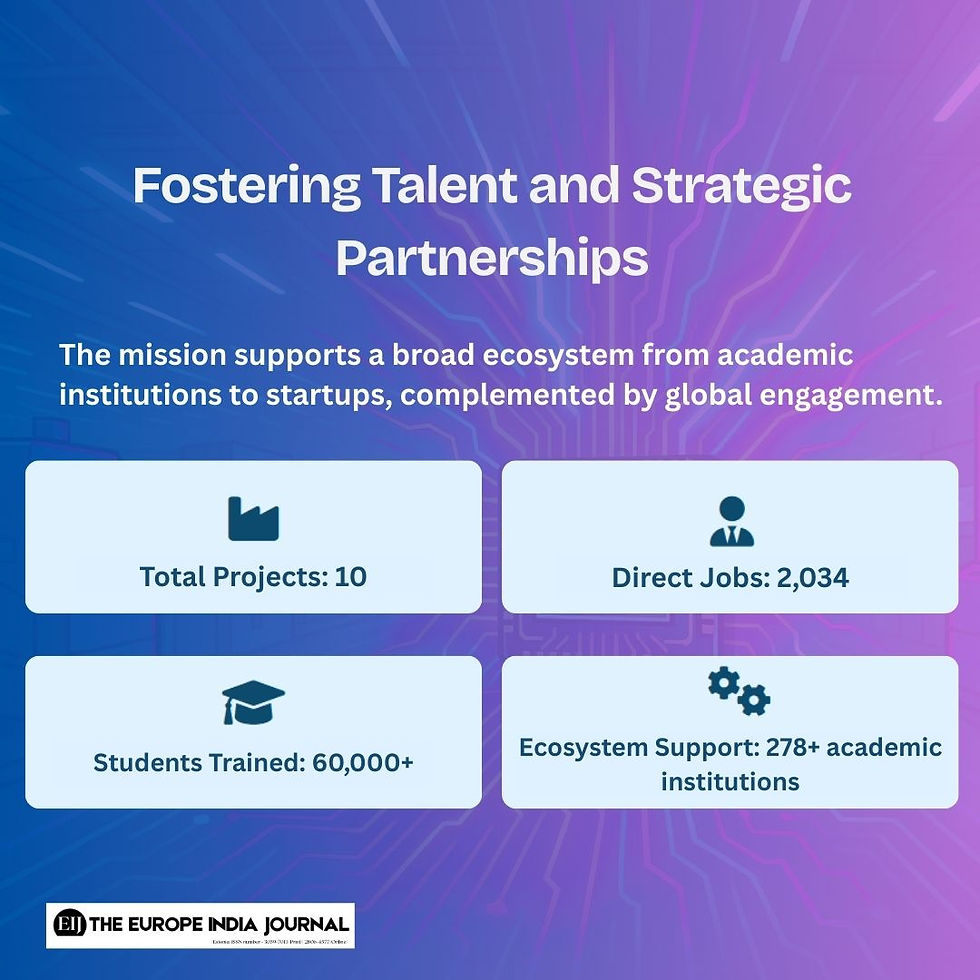
India’s semiconductor ecosystem took a remarkable stride forward as the Union Cabinet approved four new manufacturing projects in Odisha, Punjab, and Andhra Pradesh, marking a key milestone in the country’s ambition to be a leading global player in advanced electronics. This latest official announcement brings the total number of approved projects under the India Semiconductor Mission (ISM) to ten, collectively representing investments of approximately ₹1.60 lakh crore across six states.
Expansion into Compound Semiconductors & Advanced Packaging
The newly approved projects usher in India’s entrance into the realms of compound semiconductors and advanced packaging technologies, critical areas for the next generation of electronics. SiCSem Private Limited, in collaboration with UK-based Clas-SiC Wafer Fab Ltd., will establish India’s first commercial compound semiconductor fabrication unit in Info Valley, Bhubaneshwar, Odisha. This facility will focus on manufacturing Silicon Carbide (SiC) based devices, offering a production capacity of 60,000 wafers and 96 million packaged units annually. SiC semiconductors play an essential role in high-performance applications such as missiles, defence systems, electric vehicles, railway electrification, fast chargers, data centre racks, consumer appliances, and solar power inverters.
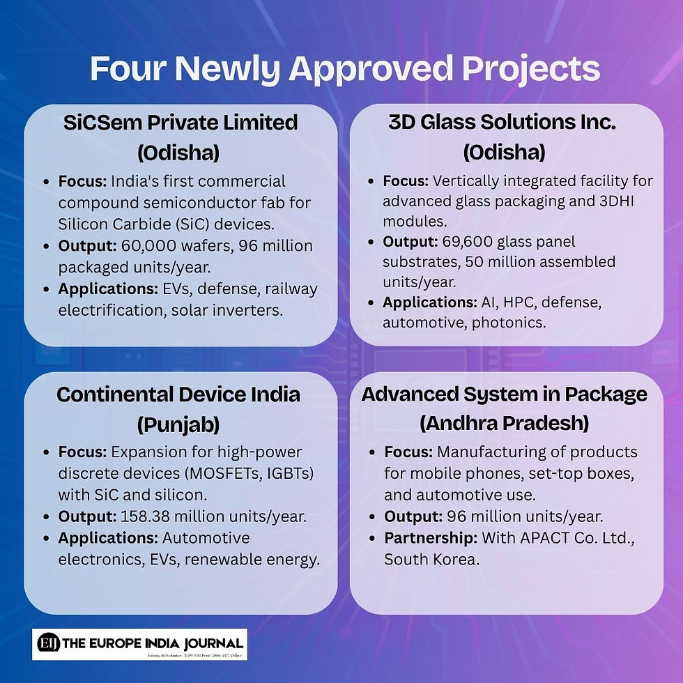
Alongside this, 3D Glass Solutions Inc. (3DGS) will set up a vertically integrated facility for advanced packaging and embedded glass substrates in Bhubaneshwar. This unit is set to introduce world-class packaging technology, featuring glass interposers, silicon bridges, and 3D Heterogeneous Integration (3DHI) modules with broad applications in defence, artificial intelligence, high-performance computing, RF and automotive, photonics, and co-packaged optics. The planned annual capacities include approximately 69,600 glass panel substrates, 50 million assembled units, and 13,200 3DHI modules.
Boost to Domestic Semiconductor Manufacturing
The expansion is not limited to Odisha. Continental Device India Private Limited (CDIL) is advancing its Mohali, Punjab facility with a brownfield expansion for manufacturing high-power discrete devices, including MOSFETs, IGBTs, Schottky bypass diodes, and transistors using both silicon and silicon carbide technologies. The projected annual output of 158.38 million units will serve India’s automotive electronics sector, particularly electric vehicles and chargers, renewable energy, power conversion, industrial applications, and communications infrastructure.
Meanwhile, Advanced System in Package Technologies (ASIP) will set up a unit in Andhra Pradesh in partnership with APACT Co. Ltd., South Korea. With an annual capacity of 96million units, the facility will manufacture products for mobile phones, set-top boxes, automotive uses, and other electronic applications.
Catalyzing Investment and Skilled Employment
Collectively, these four newly approved semiconductor projects will bring in approximately ₹4,600 crore of investment and are expected to create direct employment for 2,034 skilled professionals. As the demand for semiconductors rises in sectors like telecom, automotive, data centres, and consumer electronics, India’s proactive developments, infrastructure, and manufacturing capacity are poised to catalyse increased electronic production and generate significant indirect jobs.
Advancing Chip Design and Talent Development
These industrial projects complement the government’s support to chip design and talent development. To date, over 278 academic institutions and 72 start-ups have received infrastructural support, fostering innovation and nurturing design capabilities. More than 60,000 students have benefited from the official talent development programmes, helping to build a robust talent ecosystem for India’s electronics sector.
Strategic Importance and Sectoral Impact
The ISM’s latest approvals lay a strong foundation for innovation, import substitution, and technological self-reliance, strengthening India’s global stature in electronics manufacturing. Having the country’s first commercial compound semiconductor fab and a state-of-the-art advanced glass-based substrate packaging unit will not only diversify India’s production capabilities but also accelerate progress in industries vital to national advancement, including defence, mobility, clean energy, and digital infrastructure.
As the sector’s momentum intensifies, Indian and European stakeholders are set to convene at the EU India Leaders Conference organized by the Europe India Centre for Business and Industry (EICBI). This event serves as a prominent platform for leaders, policymakers, and technology experts from both regions to collaborate, with a dedicated focus on advancing the semiconductor sector within the EU-India corridor. By bringing emphasis to semiconductor innovation and partnership opportunities, the conference enhances dialogue and strategic engagement, supporting further growth and cooperation in this critical industry.


Comments